14 output 70 data. Select a suitable name for your project.

Ram Verilog Code Rom Verilog Code Ram Vs Rom
There is no difference or perhaps a little difference between using packed and unpacked arrays.

. Verilog RAM RTL code. Differentiate between Verilog structural dataflow behavioral design styles and how when to use them in Digital Design and Verification. Deepak Kumar Tala 6 ----- 7 module rom_using_file 8 address Address input 9 data Data output 10 read_en Read Enable 11 ce Chip Enable 12.
Initial begin display Loading rom. As follows refer to Verilog slicing link for further information. Master the basics of Verilog language for designing synthesizable digital circuits for ASIC FPGA.
Rom_using_filev 4 Function. 1 ----- 2 Design Name. Each section shows the list of Verilog-files require to implement the design in that section.
Here in this post I have written the Verilog code for a simple Dual port RAM with two ports 0 and 1. Rom_using_file 3 File Name. Always posedge clk begin if we mema.
RAM Verilog Code ROM Verilog Code. A Guide to Digital Design and Synthesis With CDROM Hardcover ed 0130449113 9780130449115. Start ModelSim from the desktop.
Create a Verilog HDL design that instantiates the function. The practical guide for every circuit designer creating FPGA designs with Verilog Walk through design step-by-step-from coding through silicon. Module ram_singleq a d we clk.
ROM in verilog If you use ROM for emulation you can use this construct for example. 13 input 70 address. Each bit in an SRAM is stored on four transistors M1 M2 M3 M4 that form two cross-coupled inverters.
Y is necessarily a constant. This storage cell has two stable states which are used to denote 0 and 1. To start memory 64-bit design simulation install ModelSim V 104a on a Windows PC and follow the steps mentioned below.
Childrens World Atlas With CDROM 9780756675844 0756675847. Real World FPGA Design with Verilog guides you through every key challenge associated with designing FPGAs and ASICs using Verilog one of. Implement synchronous RAM Random Access Memory and also provide a test-bench to validate it.
17 18 reg 70 mem 0255. So prefer using mixed block array. End else c_out.
You will see ModelSim104a dialogue window 2. Readmemh rom_imagemem test_memory. Synchronous Random Access Memory RAM implementation in Verilog.
The design uses look up tableLUT method for generating the sine wave. 234 6 40MB Read more. ROM 1 series adder 1 seven.
Reg 70 test_memory 015. 6111 Spring 2006 Introductory Digital Systems Laboratory 8 Block RAMROM Contents coe file looks like. Alwaysnegedge reset ifreset begin ROM0.
The sine wave is sampled at a pre-fixed sample rate and the values are stored in a ROM. All the design files are provided inside the VerilogCodes folder inside the main project directory. Design module single_port_sync_ram parameter ADDR_WIDTH 4 parameter DATA_WIDTH 32 parameter DEPTH 16 input clk.
Use the genmem utility to generate a memory model by typing the following command at the UNIX prompt. Following is the figure and verilog code of RAM Random Access Memory. Verilog HDL Fundamentals for Digital Design and Verification.
Which can be used to implement the design using some other software as well. The test memory has 16 locations 015 depth each of 8 bits 70 data width. End But you should use Macro from FAB if youre going to synthesize real ASIC.
Reg 40 ROM 630. Introduction to Verilog Chip Design Flow Chip Abstraction Layers Data Types Verilog Syntax Verilog Data types Verilog ScalarVector Verilog Arrays Building Blocks. The reading is done from both the ports asynchronously that means we dont have to wait for the clock signal to read from the memory.
ROM using readmemh 5 Coder. Implement combinational and sequential. To instantiate a RAM or ROM function in Verilog HDL follow these steps.
Y the start position is x and count down from x by Y. The example below shows ram_singlev a Verilog Design File that implements a 128 x 8-bit synchronous single-port RAM with common read and write addresses. This page covers RAM verilog code and ROM verilog codeIt also provides link which compares RAM vs ROM.
Specify input radix memory_initialization_radix2. The writing is allowed to only one port on the positive edge the clock. Learning to do something often involves studying what other people did.
Partitioning synthesis simulation test benches combinatorial and sequential designs and more. Coefficient Multiplier always posedge clk c RAM - flow through if c_ram_en if c_ram_wr begin c_RAMi. You probably couldnt write a decent novel if youd never read a novel.
Lastly all designs are tested using Modelsim and on Altera-DE2 FPGA board. Teach Yourself Verilog With This Tiny CPU Design. Verification ambiance may be able application System Verilog after application any accurate methodology but that will be different for every distortion of the design.
The CAD software provides automatic mapping of. The following shows a very simple simulation module using readmemh. Memory_initialization_vector 00000000 00111110 01100011 00000011 00000011 00011110 00000011 00000011 01100011 00111110 00000000 Addr 0 Addr 1 Unspecified locations if.
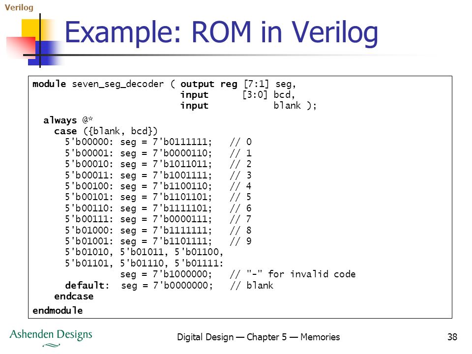
Verilog Digital Design Chapter 5 Memories 16 Example. For loading data into ROM from a file refer to this link. Home Interview Basics Design RTL VLSI Python LTE.
Set the desired design as top-level. A CD-ROM that contains Alteras Quartus CAD software comes free with every copy of the text. Chapter 3 DESIGN OF SRAM IN VERILOG 31 Design of SRAM A typical SRAM cell is made up of six MOSFETs.
Create a project by clicking Jump Start on Welcome screen 3. Reg 70 mem 1270. End Or reg 40 ROM 630.
These values are read one by one and output to a DACdigital to analog converter. This revised edition of DKs groundbreaking 2003 atlas has been refreshed with beautiful bright new maps a topic. Always posedge clk y register if y_ce begin if mult_sel begin operand1 c_out.
Create Project window pops up Fig. Figure 1 shows a. In this post I want to re-implement the same design in Verilog.

Verilog Code For Rom Youtube
2
Digital Design An Embedded Systems Approach Using Verilog Ppt Video Online Download
Design Of Rom In Verilog Youtube

Verilog Tutorial 05 Simple Rom Youtube

Ram Verilog Code Rom Verilog Code Ram Vs Rom
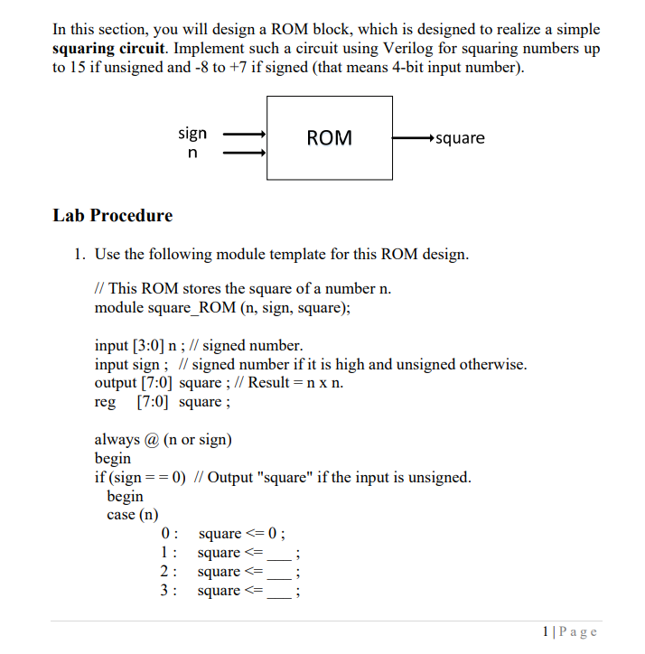
In This Section You Will Design A Rom Block Which Chegg Com

Verilog Code For Ram Youtube
0 comments
Post a Comment